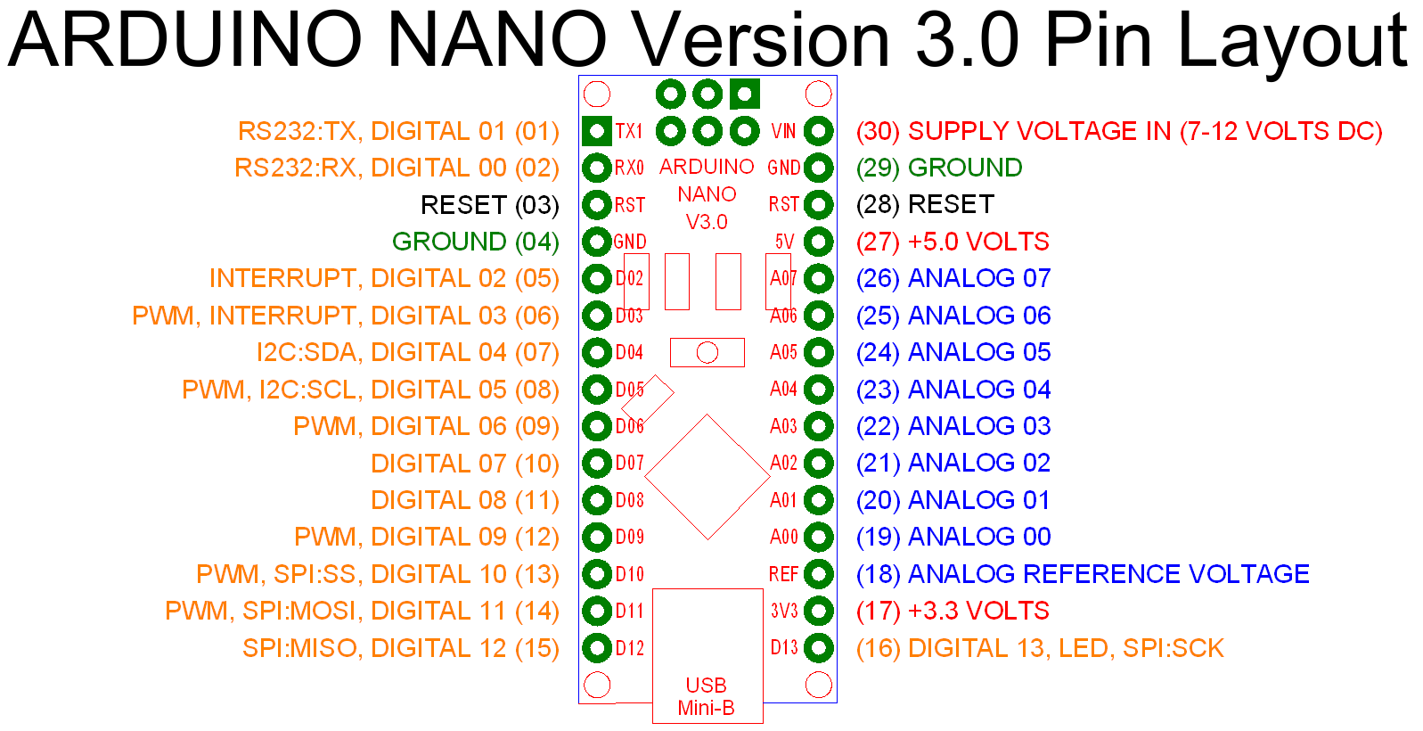
Schöne Schematic Arduino Nano V3 Fotos. This design is different from the official nano schematic, and i have not found a schematic for this. We've created a well explained, diagram based pin out if you want the reference voltage to be 0v to 3.3v, we can give 3.3v to aref pin (18th pin) by using the analogreference () function. Schematic of arduino nano 3.
㈀ ㈀ 䌀愀搀匀漀昀琀倯潲畤散︨ÿqt 4.8.2 ⡜䌀尀) 2011 nokia corporation and/or its subsidiary⡜ⴀ椀攀猀尀⤩⼊牃慥楴湯慄整⠠㩄〲㐱ㄱ㘰㤰㠱〳㸾攊摮扯੪′‰扯.
Locate d1 from the board, cut the trace at cathode side and connect cathode to vin of the regulator. Alternatively you can also remove d1 completely, but by. I chose similar components as on the official nano. 倥䙄ㄭ㐮ㄊ〠漠橢㰊਼启瑩敬⠠�䄀爀搀甀椀渀漀 一愀渀漀㈀⸀猀挀栀䌯敲瑡牯⠠�䔀䄀䜀䰀䔀 嘀攀爀猀椀漀渀 㘀⸀㌀⸀ 䌀漀瀀礀爀椀最栀琀 尀(c⥜ 㤀㠀㠀ⴀ. I made this schematic for the arduino nano 3.2 to be as close as possible to the official schematic found here. This does mean the schematic is a bit weird, as the resistors, for example, are merged into resistor arrays, meaning i had to make some. Regulated power supply used to power microcontroller and other components on the board. It has similar functionality to the arduino duemilanove, but in a dip module package. ㈀ ㈀ 䌀愀搀匀漀昀琀倯潲畤散︨ÿqt 4.8.2 ⡜䌀尀) 2011 nokia corporation and/or its subsidiary⡜ⴀ椀攀猀尀⤩⼊牃慥楴湯慄整⠠㩄〲㐱ㄱ㘰㤰㠱〳㸾攊摮扯੪′‰扯. Arduino pc6(reset) pb6cxtal1) pb7cxtal2) pdocrxd) pd1.